| |
 Image / Flash Image / Flash

 LEDs (Short Range) LEDs (Short Range)
-


 3DV Systems
Israel
Http://www.3dvsystems.com/technology/technology.html 3DV Systems
Israel
Http://www.3dvsystems.com/technology/technology.html
Contact Us
For more information about 3DV Systems and its products, and for inquiries regarding potential
partnerships and regarding careers in 3DV, please contact us using one of the following methods.
By e-mail:
info@3dvsystems.com
By mail:
3DV Systems
2nd Carmel St.
Industrial Park Building 1
P.O.Box 249
Yokneam, 20692
Israel
By fax:
+972-4-9590719
By phone:
+972-4-9599599
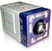
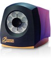
- Z-Cam
3DV Systems has developed a unique video imaging technology and camera for sensing distance
in real-time between an imaging sensor and the objects in its field of view (i.e. the objects' depth),
at high speed and high resolution. The technology, which is based on the Time-of-Flight principle,
is described thoroughly in several publications by the company's founders and engineers, and is
well protected by international patents.
Ever since 3DV released Z-CamTM, the world's first real time depth camera using this technology,
the company's primary focus has been bringing down the cost and size of its products. The product
evolution has culminated in the recent completion of the prototype of the new ZCamTM (previously
Z-Sense), a low-cost small-sized web camera to be available for sale soon, and in the nearing
launch of DeepCTM, a chipset incorporating its core depth sensing technology.
- Time-of-Flight
- Technologie
-
Http://www.3dvsystems.com/technology/tech.html#1
Technology
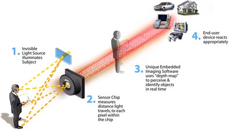
3DV Systems' image sensing technology generates distance (depth) information for each pixel or
object captured by the camera, as well as color video. The technology is based on the Time-Of-Flight
(TOF) principle. The Depth information is captured by emitting pulses of infra-red light to all
objects in the scene and sensing the reflected light from the surface of each object. All objects in
the scene are then arranged in layers according to the distance information sensed by the D pixels
in the camera, providing the Depth information in real time as standard black and white video where
the grey-level correlates to relative distance. Color data is provided using a normal color imaging
sensor. The company has filed for 22 patents related to its technology, 7 of which were granted to
date.
Fig.1 - moving light wall Fig.2 - reflected light
Fig. 3 - gating reflected light Fig. 4 - RGB and depth image
3DV's core technologies are in the 3D system level, in nano-second imaging-quality shutters based
on GaAs or Silicon, as well as in extremely fast and tightly controlled illumination. The technology
performs superior depth imaging (depth resolution of millimeters) in real-time (60 fps or more), using
little or no CPU.
Publications:
"Depth Key"
Ronen Gvili, Amir Kaplan, Dr. Eyal Ofek and Dr. Giora Yahav
SPIE Electronic Imaging 2003 Conference
Santa Clara, California
View PDF
"3D Imaging in the studio"
Dr. G. J. Iddan & Dr. G. Yahav
SPIE Vol. 4298, pp. 48.
View PDF
"3D imaging Camera for Gaming Application"
G. Yahav, G.J. Iddan & D. Mandelbaum
Submitted to IEEE 2006
View PDF
Towards and optimized 3D broadcast chain
Marc Op de Beeck, Piotr Wilinski, Christophe Fehn, Peter Kauff, Wijnand Ijsselsteijn, Marc
Pollefeys, Luc Van Gool, Eyal Ofek and Ian Sexton
SPIE vol. 4864, pp. 42
View PDF
» See document: http://www.3dvsystems.com/technology/tech.html#1
- Evolution
Product Evolution
3D video cameras by 3DV
Since it was established 3DV Systems has developed 4 generations of depth cameras. Its primary
focus in developing new products throughout the years has
been to reduce their cost and size, so that the unique state-of-the-art technology
will be affordable and meet the needs of consumers as well as of these of
multiple industries.
3D Video Camera Technology
In recent years 3DV has been developing DeepCTM, a chipset that embodies the company's core
depth sensing technology. This chipset can be fitted to work in any camera for any application, so
that partners (e.g. OEMs) can use their own know-how, market reach and supply chain in the
design and manufacturing of the overall camera capabilities. The chipset will be available for sale
soon.
3D Video Camera Technology
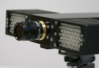
The new ZCamTM (previously Z-Sense), 3DV's most recently completed prototype camera, is
based on DeepCTM and is the company's smallest and most cost-effective 3D camera. At the size
of a standard webcam and at affordable cost, it provides very accurate depth information at high
speed (60 frames per second) and high depth resolution (1-2 cm). At the same time, it provides
synchronized and synthesized quality color (RGB) video (at 1.3 M-Pixel). With these
specifications, the new ZCamTM (previously Z-Sense) is ideal for PC-based gaming and for
background replacement in web-conferencing. Game developers, web-conferencing service
providers and gaming enthusiasts interested in the new ZCamTM (previously Z-Sense) are invited to
contact us.
As previously mentioned, the new ZCamTM (previously Z-Sense) and DeepCTM are the latest
achievements backed by a tradition of providing high quality depth sensing products. Z-CamTM, the
first depth video camera, was released in 2000 and was targeted primarily at broadcasting
organizations. Z-MiniTM and DMC-100TM followed, each representing another leap forward in
reducing cost and size.
Depth Sensing Camera
- Depuis 2000
- Previously Z-Sense
- Z-mini
- Demos
- Applications
- 3D Vision for robots
Robotics and Medical Devices
* 3D vision for robots
* 3D vision for the blind and in-body operations
* Medical diagnostics
3D Vision for Robots & Medical Diagnostics - 3D vision for the blind and in-body operations
Humans see the real world in three dimensions, or in other words as a set of objects with depth
using various 'depth cues' which include shadows, shading, movement, size; and most significantly
different and separate images for
the right and left eyes (stereoscopic vision).
While robots need to have a three dimensional vision of the world too to perform many of their
tasks, using the same 'depth cues' in robotics is difficult and ineffective.
Real-time depth capturing using 3DV's technology will make a radical change in the tasks that can
be accomplished by intelligent and cost effective robots. Activities such as Material Handling;
Assembly & Pick-and-Place; Collision Warning & Obstacle Detection; and Navigation, would be
executed much more efficiently and robustly.
Some of the robotics applications could play a role in medical devices (e.g. obstacle detection and
navigation for the blind providing a 3D view during an operation inside the body). Additionally, the
imaging technology developed by 3DV could be employed in other medical applications, primarily
in diagnostics (e.g. ophthalmic diagnostics,
IR mammography).
» See document: http://www.3dvsystems.com/applications/other.html
-
PMD Technologies
Http://www.pmdtec.com/e_index.htm
» See document: http://www.pmdtec.com/e_index.htm
- Products
PMD[vision]® Camera-Sets
Order now!
PMD[vision]® Camera-Sets are complete systems for the recording and processing of 3D data in
real time.
PMD[vision]® 1k-S, 64 x 16 pixels, contains circuitry for Suppression of Background Illumination
(SBI)
PMD[vision]® 3k-S, 64 x 48 pixels and active Suppression of Background Illumination
PMD[vision]® 19k, 160 x 120 pixels
New 3D PMD camera is available
PMD[vision]® A-sample receiver, 64 x 16 pixels for ranges up to 40m
Upon request also with 64 x 48 pixels available.
image examples of PMD[vision]® 1k-S
Data Sheet of PMD[vision]® 1k-S (pdf 361 KB)
Data Sheet of PMD[vision]® 3k-S (pdf 359 KB)
Data Sheet of PMD[vision]® 19k pdf 366 KB)
PMD[vision]® Camera
Ask for your price quotation:
phone +49 271 238 538-818 or
email sales@PMDTec.com
-
ToF measurement
Modulated NIR Light
- Canesta
http://www.canesta.com/
Sunnyvale, San Jose, CA

Canesta, Inc. Americas Headquarters
440 N. Wolfe Rd Suite 101
Sunnyvale, CA 94085
USA
Phone +1 (408) 524-1430
Fax +1 (408) 530-1527
Canesta Europe
Phone +49-(0)89-3398 5962
Canesta Detroit
445 Valleyview Drive
W. Bloomfield, MI 48323
USA
Phone +1 (248) 432-2842
Canesta Asia, Inc.
Cerulean Tower 15F
26-1 Sakuragaoka-cho
Shibuya-ku Tokyo
150-8512
Tokyo, Japan
Phone +81 [3] 5456-5318
EMPLOYMENT jobs@canesta.com
PRESS CONTACTS
Paul Michelson | Abigail Johnson
Roeder-Johnson Corporation
+1 (650) 802-1850
email.roeder-johnson.com
SALES
SUPPORT
Email: support@canesta.com
Phone (USA and Canada): (800) 348-3838
Phone (Rest of World): +1 (408) 524-1466
MORE INFORMATION
More information on Canesta's electronic perception technology and products will be distributed
through this web site as it becomes available. Common requests are addressed below:
End-users/Consumers: If you are interested in a projection keyboard, the first application of
electronic perception technology, please contact Celluon directly.
Distributors: Canesta sells its products directly to high volume manufacturers and is not seeking to
enter into distributor relationships at this time.
Educational/Academic Research Institutions and Students: Educational and academic institutions
and students have shown considerable interest in experimenting with and better understanding
electronic perception technology. Canesta believes that this type of work could lead to many new
innovative uses for the technology. Development Kits are available at a reduced price for academic
institutions that qualify.
Individual Investors: Canesta is currently a private company and does not offer shares to the
general public.
===========
Canesta was founded in April 1999, and is located in San Jose, CA. The company has filed in
excess of forty patents, 30 of which have been granted so far. Investment to date exceeds $36
million, from Apax Partners, CarlyleVenture Partners, Intel Capital, JP Morgan Partners, Korea
Global IT Fund (KGIF), TechFund Capital, Thales Corporate Ventures, and Venrock Associates.
» See document: http://www.canesta.com/
- Profile
Canesta is the inventor of a revolutionary, low-cost electronic perception technology that enables
machines and ordinary electronic devices to perceive and react to nearby objects or individuals in
real time.
When sight-enabled with Canesta's unique electronic perception chips and software, consumer,
automotive, industrial, military, and medical product scan gain functionality and ease of use not
possible in an era when such devices were blind.
Canesta believes future applications of electronic perception technology are virtually as broad as
the imagination. They may include intelligent automobile airbag systems that can sense the size
and position of an occupant to control deployment and avoid injury, a low-false-alarm security
system that could detect the difference between an intruder and normal activity, such as a pet
moving or child visiting the bathroom at night, or robotic tools that can successfully operate in a
dynamic, rather than static environment.
The first application of electronic perception technology is a projection keyboard for mobile devices,
first commercialized by Canesta in 2003. This technology was licensed to Celluon, which is now
making the solution available as an accessory and plans to offer embedded solutions for large
OEM customers seeking to incorporate the technology in their devices. Contact Celluon for more
information.
Canesta
was founded in April 1999
, and is located in San Jose, CA. The company has filed in
excess of forty patents, 30 of which have been granted so far. Investment to date exceeds $36
million, from Apax Partners, CarlyleVenture Partners, Intel Capital, JP Morgan Partners, Korea
Global IT Fund (KGIF), TechFund Capital, Thales Corporate Ventures, and Venrock Associates.
Our company is pleased to be a member of the Fabless Semiconductor Association (FSA). The
organization encourages the relationship between fabless companies and suppliers; facilitates
business partnerships; creates awareness of and promotes the fabless business model;
disseminates relevant data; and fosters standards and policies.
- Products
Canestas electronic perception technology is a patented, low cost, and practical technology that
enables machines and electronic devices to "see" by tracking nearby objects in three dimensions
in real time. Using EPT, Canesta CMOS chips emit a field of continuous field of infrared light and
measure the time it takes for that light to reflect back to the chip for every pixel. In real-time,
the
chip processes those distances to create a three dimensional image of the objects in its field of
vision.
Unlike traditional 2D "computer vision," EPT applications can supply actionable information
in real
time by observing the nearby environment in a reliable, fast, low-cost, and portable form factor.
EPT makes it possible for devices or applications of any complexity - from "lightweight" appliances,
PDAs, cell phones, or games to heavyweight vehicle control, security systems , and robotics to
perceive objects and features in the nearby environment, identify those objects, and take action in
real time.
Canesta is the leader in defining and implementing practical EPT solutions with the development of
low-cost, semiconductor-based EPT chip technology and powerful embedded image processing
software. Canesta's technology provides actionable perceptions or identifications to third-party
applications, enabling those applications to respond in a timely fashion.
Canesta's Electronic Perception Technology
- Projection Keyboard
- Electronic Perception
Technology
- CanestaVision
- CMOS Chips
CANESTAVISION CHIPS
Most people understand that light takes a finite time to travel between two points -- that photons of
light from two different stars, for example, may have started their journeys years, or even millennia
apart. Since light travels essentially at a constant speed, if you know the time, you can calculate
the distance.
The light illuminating each individual pixel in an image sensor comes from a different feature in the
scene being viewed. Canesta recognized that if you could determine the amount of time that light
takes to reach each pixel, you then could calculate with certainty the exact distance to that
feature. In other words, you could develop a three-dimensional "relief" map of the surfaces
in the
scene. In three dimensions, objects previously indistinguishable from the background, for example,
metaphorically "pop" out. For a broad class of applications, this proves extremely helpful
in
reducing the mathematical and physical complexity that has plagued computer vision applications
from the start.
In a recently-granted U.S. patent, Canesta describes several of its inventions for "timing"
the travel
time of light to a unique, new class of low-cost sensor chips.
Fundamentally, the chips work in a manner similar to radar, where the distance to remote objects
is calculated by measuring the time it takes an electronic burst of radio waves to make the round
trip from a transmitting antenna to a reflective object (like a metal airplane) and back. In the case
of
these chips, however, a burst of unobtrusive light is transmitted instead.
The chips, which are not fooled by ambient light, either then time the duration it takes the pulse to
reflect back to each pixel, using high speed, on-chip timers in one method, or simply count the
number of returning photons, an indirect measure of the distance, in another.
In either case, the result is an array of "distances" that provides a mathematically accurate,
dynamic "relief" map of the surfaces being imaged. The image and distance information is then
handed off to an on-chip processor running Canesta's proprietary imaging software that further
refines the 3-D representation before sending it off chip to the OEM application.
Performance of a Time-of-Flight Range Camera for Intelligent Vehicle Safety Applications
An Occupant Classification System Eigen Shapes or Knowledge-Based Features
- Measuring the time delay of modulated infrared light from an active emitter
- Light source constructed from a bank of infrared LEDs (or laser diodes)
- A lens system for the detector chip
- A detector chip with 160×120 phase-sensitive pixels fabricated on standard CMOS
» See also: CMOS Chips
- 2006
- S. Hsu, S. Acharya, A. Rafii and R. New,
(Canesta, Inc.), Performance of a
Time-of-Flight Range Camera for Intelligent
Vehicle Safety Applications. AMAA06
- Http://www.youtube.com/watch?v=JTE8S3AF0dc
» See document: http://www.youtube.com/watch?v=JTE8S3AF0dc
- CSEM
Swiss Center for Electronics and
Microtechnology, Inc.
http://www.csem.ch/
http://www.csem.ch/
CSEM SA Headquarters
Centre Suisse
d'Electronique et de
Microtechnique SA
Rue Jaquet-Droz 1
P.O. Box
CH-2002 Neuchâtel
Tel. +41 32 720 5111
Fax +41 32 720 5700
CSEM Zurich
Technoparkstrasse 1
CH-8005 Zürich
Tel. +41 44 497 1411
Fax +41 44 497 1400
CSEM Basel
Mattenstrasse 22
P.O. Box
CH-4016 Basel
Tel. +41 61 690 6011
Fax +41 61 690 6000
CSEM Alpnach
Untere Gründlistrasse 1
CH-6055 Alpnach Dorf
Tel. +41 41 672 7511
Fax +41 41 672 7500
CSEM Landquart
Schulstrasse 1
CH-7302 Landquart
Tel. +41 81 330 0970
Fax +41 81 330 0971
===================================
PROFILE
CSEM, the Swiss Center for Electronics and Microtechnology, Inc., is a privately held research and
development company active in:
* Applied Research
* Product Development
* Prototype and Low-volume Production
* Technology Consulting
Its main fields of activity are micro- and nanotechnologies, microelectronics, systems engineering,
microrobotics, photonics, information and communication technologies.
In providing its high-tech know-how and technological expertise, CSEM strives to anticipate the
future needs of different markets in terms of new technologies and offers its services to industrial
customers. It also develops its own commercial activities either together with existing companies
or through the creation of spin-offs and start-up companies and actively contributes to developing
Switzerland as a high-tech industrial location.
In July 2007, a major of the Neuchâtel Observatory was integrated into CSEM to continue to
develop space-related technologies. CSEM microsystems and miniaturization competences will be
a clear advantage in terms of new developments in this area.
Furthermore, CSEM opened new research centers in Landquart aimed at developing new
technologies and competences in nanomedicine, and in Basel specialized in polymers optics and
optical microsystems.
CSEM operates from its headquarters in Neuchatel and also has centers in Zurich, in Basel, in
Landquart and at Alpnach, near Lucerne. It is also internationally active, in many European
countries as well as overseas. CSEM is pursuing its geographical expansion strategy on a national
as well as an international level. This growth offers medium- and long-term stability, essential in
an
R&D environment.
2007 was a year of success for the CSEM's human resources: Thanks to its exemplary equal
salary policy, CSEM obtains the "Equal Salary" label that certifies the respect of equal
compensation for men and women .
At the end of 2007, the total number of employees at CSEM was 348 of which 26 were Ph.D
candidates. Additionally, approximately 500 people are employed by the 26 spin-offs and start-ups
created to date. These companies have directly generated over 500 highly qualified positions, and
attracted over 170 million CHF venture capital investment for an annual turnover in 2006 of over 100
million CHF.
=========================
» See document: http://www.csem.ch/
- MESA Imaging AG
http://www.mesa-imaging.ch/
Zurich, Switzerland
http://www.mesa-imaging.ch/
About MESA Imaging
MESA Imaging AG was
founded in July 2006
to commercialize the world-leading 3D Time-of-Flight
depth mapping technology developed by MESA founders while at CSEM.
MESA has commercialized image sensor technology capable of capturing in real time 3-dimensional data
sets (known as depth maps) using a single, compact, solid-state camera.
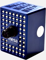
Along with its award-winning SwissRanger SR-3000 product, MESA is able to draw on its
extensive experience to develop customized imaging and camera solutions.
MESA has been shipping product since its founding, and its products are widely recognized as the
highest performance in its class. Privately financed, with headquarters in Zurich, Switzerland,
MESA is developing innovative solutions for a wide variety of markets:
* Video Gaming
* Machine Vision
* Robotics
* Medical and Biometrics
* Farm Automation
======================
» See document: http://www.mesa-imaging.ch/
- TOF from Modulated Sinewave IR
- SwissRanger
» See also: Principle
- SwissRanger SR-3000
SwissRanger SR3000
The SR3000 is a general purpose range imaging camera. The standard product can easily be
connected to a computer via USB 2.0, enabling straightforward measurement of real-time depth
maps. Designed for operation under indoor lighting conditions, the compact unit is offered with a
complete visualization software program.
Features
* Captures the 3D scene in real-time at video frame rates
* QCIF resolution (176 x 144 pixels)
* Resolution down to sub-centimeters in short range applications.
* Built-in optics (bandpass and lens system)
* Built in background light suppression
* USB 2.0 interface
* Direct Cartesian coordinate output: x, y and z
Specifications
Model No. SR3000
Pixel array resolution 176 x 144 pixels
Field of view 47.5 x 39.6 degrees
Non-ambiguity range 7.5 m (for 20MHz modulation)
Interface USB2.0
Optical lens f/1.4
Illumination power (optical) 1 W (average power) at 850nm
Camera casing 50 x 67 x 42.3 mm (aluminum)
Power 12 V, 1A
Operating temperature -10°C to +50°C
Output data x, y, z (coordinates), i (intensity)
Effective resolution (reference: imager's central pixel) 2
Operating Range [meters] 0.3 1 2 3
X-Y Resolution (one pixel) [mm] 1.5 5.0 10.0 15.0
Distance Resolution [mm] 2.5 6 13 22
[1 ]Frame rate is variable, and is dependent on user-defined settings.
Included with purchase:
Hardware:
* SR3000 camera unit
* USB2.0 cable
* Power supply
* Power supply cable
* CD with all manuals, visualization software, and drivers.
Software:
* Drivers for Windows, Linux, MacOS
* Demo software (Windows)
* Sample code in C/C++ (Windows)
* Viewer application for MacOS
* Matlab user interface
» See document: http://www.mesa-imaging.ch/prodview3k.php
- USB 2.0,
- QCIF resolution (176 x 144 pixels)
- Output data x, y, z (coordinates), i (intensity)
- Direct Cartesian coordinate output: x, y and z
- Field of view 47.5 x 39.6 degrees
- Power 12 V, 1A
- Operating temperature -10°C to +50°C
- SwissRanger SR4000
SwissRanger SR4000
The SR4000 is an optical imaging system which provides real time distance data at video frame
rates.
Based on the time-of-flight (TOF) principle, the camera employs an integrated light source. The
emitted light is reflected by objects in the scene and travels back to the camera, where the precise
time of arrival is measured independently by each pixel of the image sensor, producing a per-pixel
distance measurement.
Designed for indoor operation, the SR4000 is easily connected to a computer or network via the
USB2.0 or Ethernet interface, enabling creation of real-time depth maps.
Representing the 4th generation of time-of-flight cameras designed by MESA, the SR4000 provides
stable distance information in a robust, reliable hardware package measuring 65 x 65 x 68mm
(USB version).
Features
* Captures the 3D scene in real-time at video frame rates
* Self calibrating optical design yields stable measurement results
* Solid-state design
* 176 x 144 pixel array (QCIF)
* In-pixel background light suppression
* USB 2.0 or Ethernet interfaces
* Continuous or external trigger acquisition modes
* Multi-camera operation using Coded Binary Sequence modulation
* Eye-safe LED illumination
* Robust industrial grade housing
* User selectable parameters, including focus, frame rate (exposure time), and
continuous vs.
trigger mode operation
Performance Specifications
Pixel Array Size 176 (h) x 144 (v) QCIF
Field of View 43.6° x 34.6° Lens:
F# 1.0 , f=10mm
Angular Resolution 0.23° Center pixel
Illumination Wavelength 850nm Central wavelength
Modulation Frequency 30 MHz Default setting
Modulation Format Sinusoidal or CBS CBS
available in 4Q2008 release
Operating Range 0.3 to 5.0 meters With standard
settings
Distance Accuracy +/-1cm z-direction, single
pixel
Repeatability < 5mm at range up to 2 meters Single
pixel (1?); 50% reflective object
Frame Rate Up to 54 FPS Camera setting dependent
Communication Interfaces USB2.0
Fast Ethernet (100 Mb/s)
Operating Systems Windows XP, Vista, Linux, MacOS
Power Consumption 0.8 A @ 12V
Mechanical / Environmental
Operating Temperature +10°C to +50°C Ambient,
with adequate heat sinking
Storage Temperature -20°C to +70°C
Dimensions 65 x 65 x 68 mm USB2.0 version
65 x 65 x 90 mm Ethernet version (includes
connector)
Industrial Rating IP-54 USB version, excluding
connector
IP-54 Ethernet version, with proper
connector
EMI Rating Class A
Case Material Anodized Aluminum
Window Material Polycarbonate Illumination
Cover
Coated Borofloat Glass Objective Cover
Mounting Holes 4 x M4; 2 x 4H7; 1 x 1/4
Notes
1. The SR4000 is designed for operation in indoor environments.
2. Camera should be properly attached to a heat sink during operation.
3. Beta release; final industrial ratings upon completion of qualification.
4. All specifications are subject to change.
» See document: http://www.mesa-imaging.ch/prodview4k.php
-
Beta release;
- Time-of-flight (TOF) principle
- Solid-state design
- Captures complete 3D scenes at video frame rates
- 176 x 144 pixel array (QCIF)
- Field of View 43.6° x 34.6°
- USB 2.0 or Ethernet interface
- Eye-safe LED illumination
- INDOOR Applications
- 5X overall improvement in distance measurement performance
- External trigger
- FAQ
Frequently Asked Questions
What are the differences between the SR3000 and SR4000?
The SR4000 represents a complete redesign, including custom designed optics, housing, and all
electronics. The SR4000 sensor chip employs MESAs 4th Generation pixel architecture, offering a
5X overall improvement in distance measurement performance.
As a fully enclosed, dust and moisture tight mechanical design (with use of proper connectors and
cables), the SR4000 is fit for use in industrial environments. The SR4000 does not have an
embedded fan like the SR3000. Mechanically the SR4000 has an entirely new form factor which is
not backwards compatible with the SR3000.
A key design feature of the SR4000 is an integrated feedback system that allows the camera to
continually self-calibrate, removing a large portion of the distance error that might occur from
variation in environmental conditions or as a result of aging of components.
Standard with the SR4000 is the choice of interfaces (USB2.0 or FastEthernet) and an external
trigger.
What is the measurement principle of the 3D-TOF technology by MESA?
The distance of an object is measured by determining the phase-shift between a continuously
modulated sine wave that is emitted and the received, reflected signal. Compared to a pulsed
measurement approach, this can be implemented at the pixel level on an area image sensor.
What kind of active illumination elements are used? Is it eye safe?
Illumination is provided from solid-state infrared LEDs in both the SR3000 and SR4000.
Current products use the LEDs that are inherently eye safe and belong to Laser Class 1
based on DIN EN 60825.1.
What are the limits in distance accuracy?
The measurement precision is determined by the amount of light which is reflected from the scene
back to the imager chip. As a general rule of thumb when operated indoors, the distance accuracy
is approximately 1% of the full range. The distance accuracy can be improved by increasing the
modulation frequency or optical power, or by reducing the frame rate.
What is a "non-ambiguity range"?
When sine wave modulation is used, one can only distinguish phase shifts below 2-pi
unambiguously. Above the 2-pi value, there is phase wrapping. For example, at 20MHz modulation,
an object at a range of 8m and one at 0.5m produce the same phase shift - and thus the same
distance value. Recently development modulation schemes overcome this ambiguity via the use of
binary coded sequences.
Can the non-ambiguity range be extended?
A reduction of the modulation frequency can extend this range. However, the measurement
resolution and precision will also be degraded since they are directly influenced by the modulation
frequency. Note that for the SR3000 and SR4000, different calibration routines are used.
SR3000: 20MHz / 7.5m range
SR4000: 30MHz / 5.0m range
Can the modulation frequency be increased further?
The SR4000 employs a new sensor technology that is capable of operation at up to 80MHz, though
in the standard product, 30MHz is the default setting. Future releases will support higher speed
operation.
How does bright background light influence the distance measurements?
Bright background light may saturate the electronics at the pixel level and hence prevent the
sensor from taking a distance measurement. MESAs current products are designed for indoor
operation, and the effect of direct sunlight upon the scene of interest may prevent proper operation.
How does distance influence the measurement accuracy?
The reflected light power decreases with the square of the distance to an object. Hence if you
double the working distance you get only one-fourth of the original light power back to the sensor.
If
no other settings are changed, this will lead to the distance accuracy being degraded by at least a
factor of four.
Are your cameras temperature stabilized?
The SR4000 does not include a fan, which is made possible by a much more efficient sensor chip
(requiring less illumination) and an industrial grade housing. Even so, proper mounting techniques
to a suitable heat sink to ensure heat removal are recommended.
The SR3000 has an internal fan is used to maintain a stable operating temperature within the
camera.
- Principle
- 3D-TOF technology by MESA = Phase-shift between a
continuously modulated sine wave
-
Eye safe
What kind of active illumination elements are used? Is it eye safe?
Illumination is provided from solid-state infrared LEDs in both the SR3000 and SR4000.
Current products use the LEDs that are inherently eye safe and belong to Laser Class 1
based on DIN EN 60825.1.
- Illumination is provided from solid-state
infrared LEDs
- Laser Class 1 (Based on DIN EN 60825.1)
-
Non-ambiguity range
Can the non-ambiguity range be extended?
A reduction of the modulation frequency can extend this range. However, the measurement
resolution and precision will also be degraded since they are directly influenced by the modulation
frequency. Note that for the SR3000 and SR4000, different calibration routines are used.
SR3000: 20MHz / 7.5m range
SR4000: 30MHz / 5.0m range
-
Accuracy = 1% of range (indoor)
- HowToBuy
Bank Details:
Credit Suisse
Rue de Seyon 12
CH-2001 Neuchâtel
Clearing # 0531
Swift code : CRESCHZZ20A (for all currencies)
(If payment in euros):
Account No : 0531-647401-62
IBAN : CH21 0483 5064 7401 6200 0
(If payment in CHF)
Account No : 0531-647401-61
IBAN : CH55 0483 5064 7401 6100 0
(If payment in US Dollars)
Account No: 647401-62-1
IBAN: CH91 0483 5064 7401 6200 1
MESA does not accept the use of credit cards.
Japan - MESA products are exclusively distributed in Japan by Clavis Corporation.
Clavis Japan Corporation
2-11-16 Kiyomidai, Kisarazu, Chiba 292-0045 JAPAN
phone +81-438-23-2344
fax +81-438-20-2377
sales@j-clavis.co.jp
www.j-clavis.co.jp
-
PMD Technologies GmbH
http://www.pmdtec.com/e_index.htm
Siegen, Germany
http://www.pmdtec.com/e_index.htm
PMDTechnologies GmbH
Am Eichenhang 50
D-57076 Siegen
Germany
phone +49 271 238 538-800
fax +49 271 238 538-809
mail info@PMDTec.com
========
Realised Visions
1996 :: First PMD patents granted
1997 :: Realisation of PMD using CMOS Founding of S-Tec GmbH
1998 :: 1D-PMD demonstration unit produced
1999 :: 2D-PMD demonstration unit produced
2001 :: First 3D-PMD camera worldwide produced
2002 :: Founding of PMDTechnologies GmbH
Takeover of S-TEC GmbH
Nomination
for the "German Future Award "
2003 :: PMD[vision] ® 1k-S with 64 x 16 pixels
2004 :: PMD[vision] ® 19k with 160 x 120 pixels
2005 :: efector pmd wins HERMES AWARD 2005
market launch of efector pmd
PMD[vision] ® 3k-S with 64 x 48 pixels
2006 :: PMD[vision] ® A-Sample with 64 x 16 pixels,
A-Sample for automotive outdoor & interior
applications
2007 :: Introduction of PMD[vision] ® evaboard
==================
» See document: http://www.pmdtec.com/e_index.htm
- Principle
Complex Measuring tasks made easy
PMDTec has developed a new generation of "Smart-Pixel" sensors - Photonic Mixer Device [PMD]
- to capture the complete 3D scene in real time. With these new semiconductor components, it is
possible to "perceive" distance in addition to the common grey level values.
A modulated optical signal sent by a transmitter, such as an invisible infrared light source,
illuninates the scene to be measured. The reflected light enters the PMD sensor, which is also
connected to the modulation source. The electrons converted into photons are separated inside the
optically sensitive area of the semiconductor by the so-called "mobile charge carrier" in
relation to
the reference signal.
A comparison between the optical and electrical reference signals yields an output signal which
carries the desired 3D information.
The big advantage of a PMD system is the efficient Suppression of Background Illumination (SBI)
[such as incidental solar radiation]. The active transmitter signal can be filtered from the ambient
light and therefore allows for robust measurement even under difficult environmental conditions.
- Smart-Pixel" sensors - Photonic Mixer Device [PMD]
- Possible to "perceive" distance in addition to the common grey level values.
- Optical signal sent by a transmitter, such as an invisible infrared light source
- Suppression of Background Illumination (SBI)
- Products
- 3D Cameras
PMD[vision]® Camera-Sets

PMD[vision]® Camera-Sets are complete systems for the recording and processing of 3D data in
real time.
PMD[vision]® 1k-S, 64 x 16 pixels, contains circuitry for Suppression of Background Illumination
(SBI)
PMD[vision]® 3k-S, 64 x 48 pixels and active Suppression of Background Illumination
PMD[vision]® 19k, 160 x 120 pixels
New 3D PMD camera is available
PMD[vision]® A-sample receiver, 64 x 16 pixels for ranges up to 40m
Upon request also with 64 x 48 pixels available.
image examples of PMD[vision]® 1k-S
Data Sheet of PMD[vision]® 1k-S (pdf 361 KB)
Data Sheet of PMD[vision]® 3k-S (pdf 359 KB)
Data Sheet of PMD[vision]® 19k pdf 366 KB)
PMD[vision]® Camera
Ask for your price quotation:
phone +49 271 238 538-818 or
email sales@PMDTec.com
- PMD[vision]® 1k-S, 64 x 16 pixels, contains circuitry for Suppression of Background Illumination (SBI)
- PMD[vision]® 3k-S, 64 x 48 pixels and active SBI
-
PMD[vision]® 19k, 160 x 120 pixels
- Sensors
3D Time-of-Flight
PhotonICs® PMD 1k-S, with 64 x 16 pixels, is a high performance, low-power 3D video image
sensor for time-of-flight distance measurement applications. With its panorama image format, it is
ideally suited for wide angle automotive and navigation applications.
The PhotonICs® PMD 3k-S, with 64 x 48 pixel and active suppression of background illumination is
very useful for industrial applications.
The PhotonICs® PMD 19k is a high speed, high resolution, low-power 3D video image sensor for
time-of-flight distance measurement applications. With its 4:3 image format (QQVGA) it is ideally
suited to 3D visualisation, virtual reality and man-machine interface applications.
New: PMD[vision]® evaboard, with one of the above mentioned sensor chips. You will be able to
adapt a PMD system to your own needs.
PhotonICs® PMD 19k
-
 Panasonic Panasonic
-
NEW 2009 - Panasonic's new 3D range sensor functions in
direct sunlight
Panasonic's new 3D range sensor functions in direct sunlight
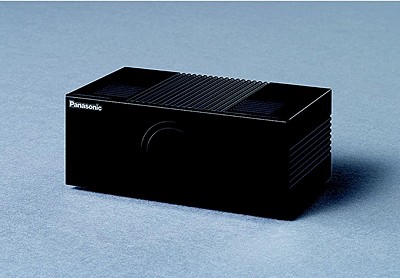
Perhaps you're looking for a way to track potential cat burglers, give your robot some spacial
sense, make your UIs a little more interactive, or you simply want to keep an eye on your
"compound." Panasonic has just released detailed specs for its 3D range sensor -- the first,
it
says, to work in direct sunlight. Exhibited at CEATEC 2008, the device emits light from several
dozen LEDs to track the movements of any object in its view. The company's previous 3D range
sensor didn't function well (if at all) in bright light, but the equipment now compensates for
"extremely bright ambient light" by measuring it and eliminating it from the equation. Can't
wait to
track your loved ones' every movement? The 24 volt, USB 2.0 sensor is slated for an April 1, 2009
release.
» See document: http://www.engadget.com/2008/10/23/panasonics-new-3d-range-sensor-functions-in-direct-sunlight/
- April 1, 2009 release
- The 24 volt, USB 2.0 sensor
- Exhibited at CEATEC 2008
- Emits light from several dozen LEDs to track
-
Work in Direct sunlight
- Feedback
- Dean @ Oct 23rd 2008 10:54AM
- Well, it's not exactly the first. PmdTec
(http://www.pmdtec.com/) makes a 3D range
sensor that works pretty well in sunlight.
- If this comes in cheaply (
Laser pulsé + ToF
|

 Trop cher